Features
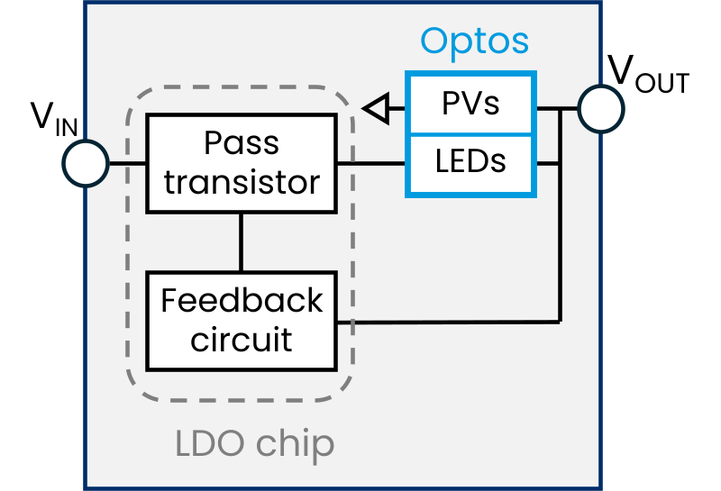
Polaris Semiconductor’s pioneering technology enables DC power management with the low noise, compactness and simplicity advantages of linear regulators but with dramatically higher efficiency. This entirely linear technology eliminates the EMI effects associated with switching alternatives, simplifying circuit design, PCB layout and reducing risks of a costly redesign. Polaris Semiconductor voltage regulators support even the most demanding, low-noise applications, including RF circuits, precision sensing, scientific instrumentation, low-noise imaging, medical devices, and many more. Radiation tolerant versions also suit demanding applications in harsh environments. The inductor-less, switching-free topology uses photons generated within proprietary optocoupler chips to unlock much higher efficiency than conventional LDOs. This simplifies thermal design and reduces electrical losses, increasing system performance without introducing noise and footprint tradeoffs.
DC Buck Voltage Regulators
Core Values
Smashing Efficiency Limits
Polaris Semiconductor voltage regulators typically deliver between 1.2 to >2X higher efficiency than a linear regulator, depending on voltage step. This greatly expands the range of applications where linear regulators can be employed, slashing heat generation and reducing current consumption.
Ultra-High PSRR & Low Noise
Polaris Semiconductor voltage regulators leverage a proprietary photonic technology that enables the clean, ripple-free output of a linear regulator but with much higher efficiency. This technology can match the noise specifications of the best available linear regulators and help reduce solution size, BoM and design complexity in many applications.
Minimal Footprint and BoM
Polaris Semiconductor voltage regulators require no inductors and only a handful of small passives to operate. Their QFN packages are compact (36-49mm² area) and low profile (0.8mm height), making them ideal for space constrained applications with demanding power integrity requirements.
Product Families
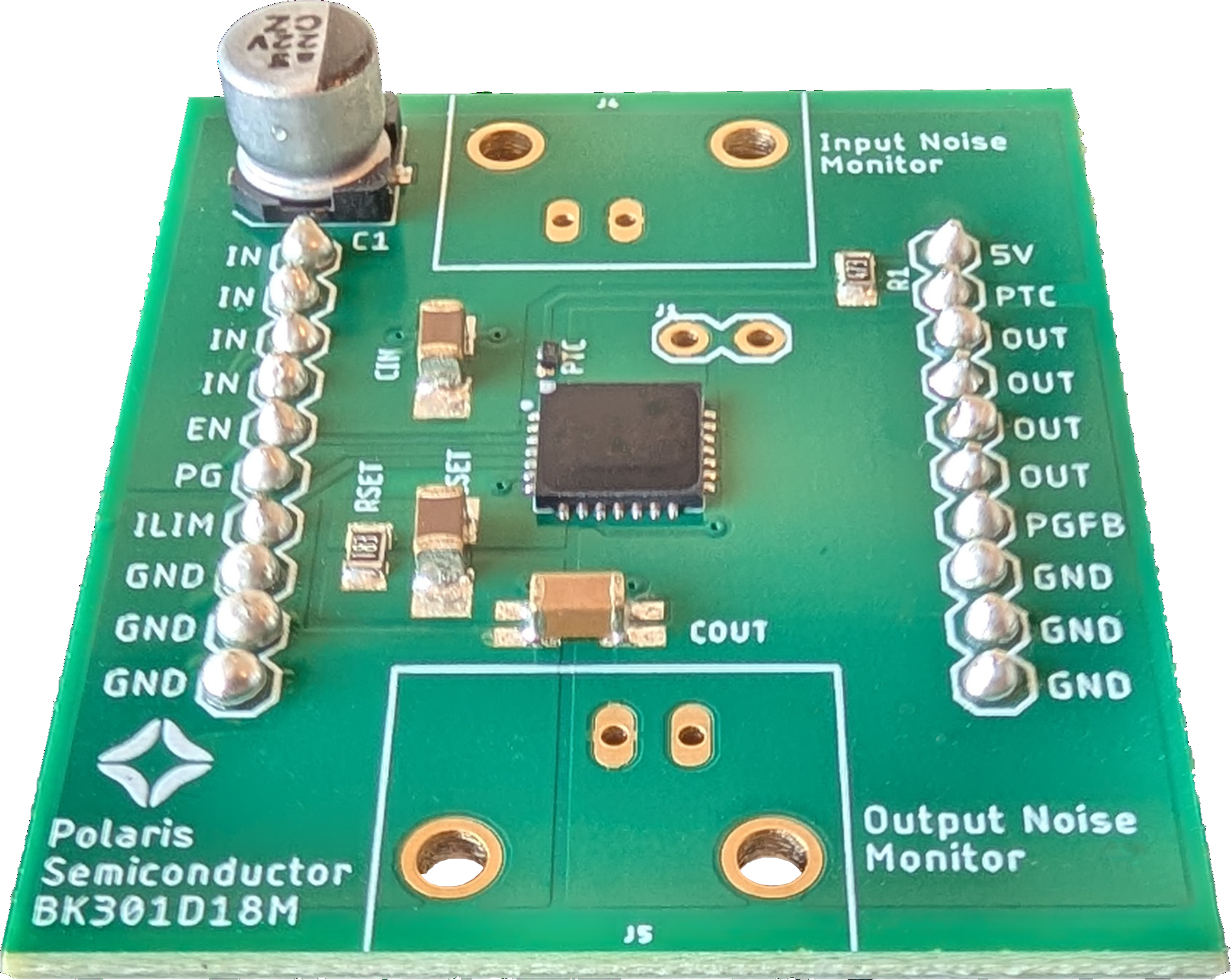
We offer three families of buck DC voltage regulators. Key performance attributes are summarized in the table. Product pages can be accessed by clicking on each device family below. Full datasheets are available upon request. All products are also available on evaluation boards.
If you don’t see a product that suits your application, get in touch as we also offer custom designs.
| Device Family | Max IOUT (mA) | Max VIN (V) |
Min VOUT (V) | PSRR @ 1 kHz |
TID 1krad (Si) |
|---|---|---|---|---|---|
| BK19 (RHA) | 900 | 20 | 1.2 | 75 dB | 200 |
| BK29 | 1500 | 26 | 1.2 | 65 dB | 200 |
| BK30 | 500 | 20 | 0 | >100 dB | TBD |
| RHA denotes the use of a radiation hardness assured LDO |
|||||
BK19 | Radiation Hardness Assured
LDO Tech: RH1965
Assured 200kRad @ 50Rad/s
Applications
Rad Hard Satellite Pwr
Clean Analog Supply
Efficient PoL Regulator
LDO Tech: MIC29152
Low ground current
Applications
Rad Tolerant Satellite Pwr
Clean Analog Supply
Battery-Powered Systems
Efficient PoL Regulator
LDO Tech: LT3045
RMS Noise < 2μV
Applications
RF & Analog Specialist
High-Precision Data Conv.
Scientific Instrumentation
Medical Devices
Efficient PoL Regulator
Finding the Right Buck Regulator Product
You can contact us with your desired regulator specifications, or explore the details below to find the best device for your application.
Step 1: Choose the Right Product Family
Each product family features a distinct low-dropout (LDO) linear regulator, co-packaged with our patented high-efficiency PV-output optocouplers. This innovation recycles power typically lost in conventional regulators, delivering significantly higher efficiency while preserving LDO benefits. Our product families are tailored for different performance requirements, such as ultra-low noise, high current, or radiation hardness. Refer to the Product Summary section to learn about the unique attributes of each series.
Step 2: Select Your Output Voltage Range
Our devices feature adjustable output voltages tailored for different ranges: 0–2V, 2–4V, or 4–5V. Within each output voltage range multiple products are available, each optimized for superior performance in different aspects, such as noise, output current, and radiation, as well as variants optimized for different input voltage ranges.
Step 3: Select Your Input Voltage Range
Our various device configurations are designed for peak optocoupler-enhanced performance within specific input voltage ranges. The last character of the Product ID indicates the input voltage range that the device has been optimized for:
L: Lowest input voltage range
M: Medium input voltage range
H: High input voltage range
E: Extended input voltage range
Devices with IDs ending in “V” support multiple input voltage ranges, selectable via board-level pin connections. All our devices can also be operated as conventional LDOs in “LDO Mode”
Contact Us
Contact us for detailed datasheets, evaluation samples, and SPICE models today!


